
With only about ten days left before NVIDIA officially presents its new range of GeForce RTX 50 Series graphics cards, the RTX 5090 seems to have been surprised in its simplest form. Photos of its bare PCB and chipset have indeed appeared, revealing some juicy details about this very high-end graphics card.
A monstrous chipset for a super-powerful graphics card
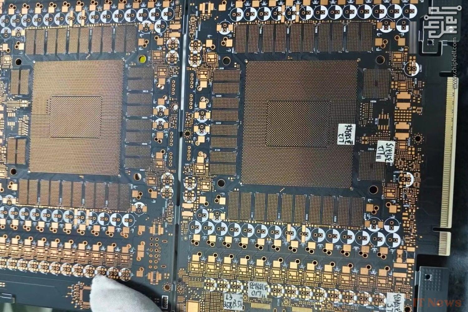
More precisely, the photo of the PCB of this GeForce RTX 5090, completely devoid of any components, confirms certain characteristics of the card. The 16 slots around the GPU are intended to accommodate as many GDDR7 memory chips, which allows capacities of 32 GB, 48 GB or 64 GB, depending on the type of VRAM chips used. The size of the PCB and the lack of “NVIDIA” wording suggest that this is a PG145 reference design, not a Founders Edition model.
The PCB also has a slot for a single 16-pin 12V power connector, confirming that the RTX 5090 complies with the PCIe 6.0 electromechanical specification. The GPU slot is particularly large, with an estimated 3776 mm² (64x59 mm). Finally, the card appears to use a PCI-Express 5.0 connector.
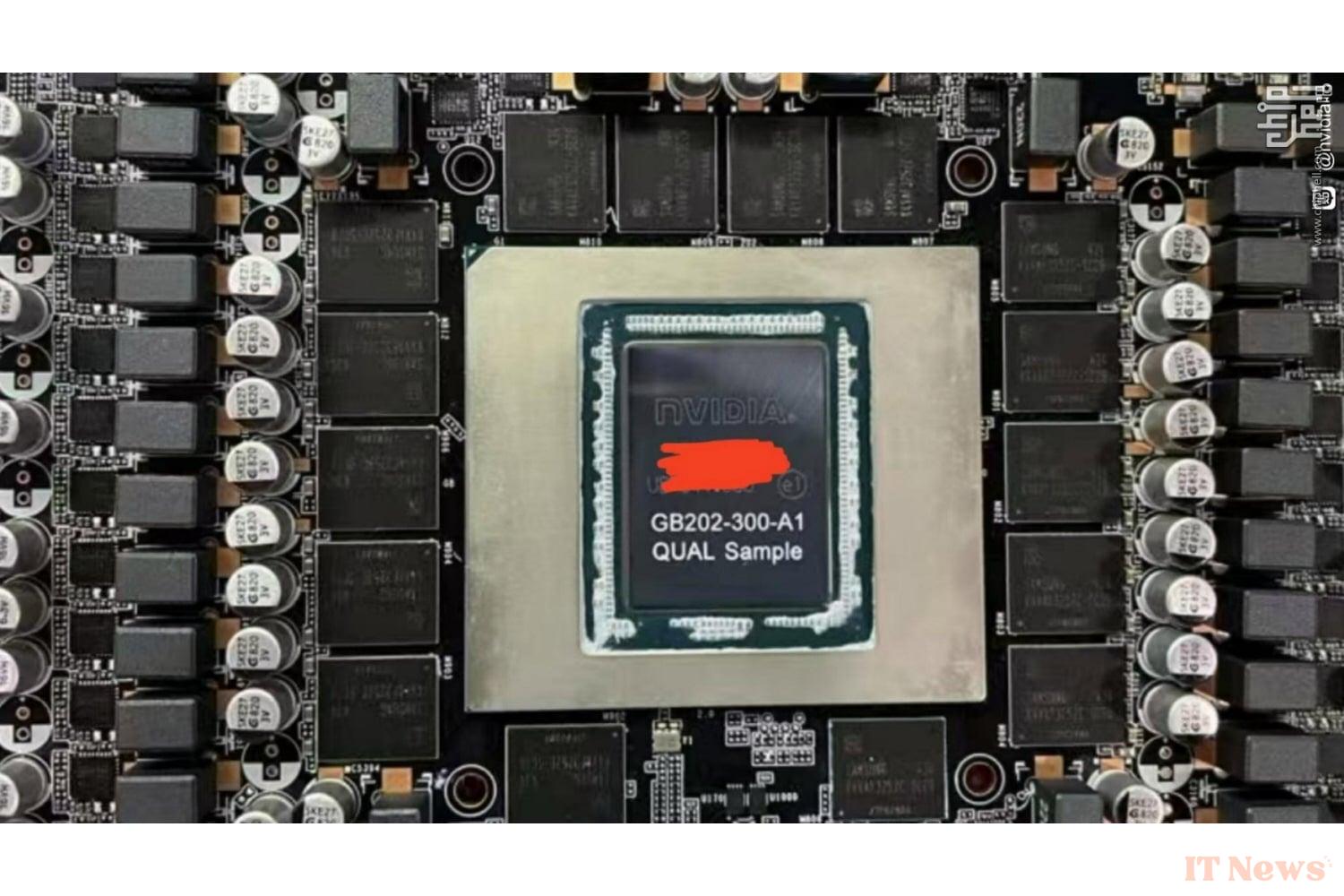
The second shot confirms the previous assumptions, with the presence of 16 GDDR7 memory chips apparently manufactured by Samsung. With an expected speed of 28 Gbps and a 512-bit memory bus, the available bandwidth would indeed reach 1792 GB/s as hoped. The GB202-300-A1 chipset – in Qualification Sample version, therefore theoretically close to the final version – is also revealed. With dimensions estimated at 24x31mm, or a surface area of 744 mm², this Blackwell GPU would be one of the most imposing offered by NVIDIA for the consumer market, since the GPUs of the RTX 2080 Ti (754 mm²) and TITAN V (815 mm²).
The GeForce RTX 5090 should not use all the power of the GB202 chipset: only 21760 CUDA cores would be activated out of the 24576 cores that a complete GB202 would have. Enough to leave room for a hypothetical RTX 5090 Ti or Super in the coming months…
Source: Chiphell


0 Comments