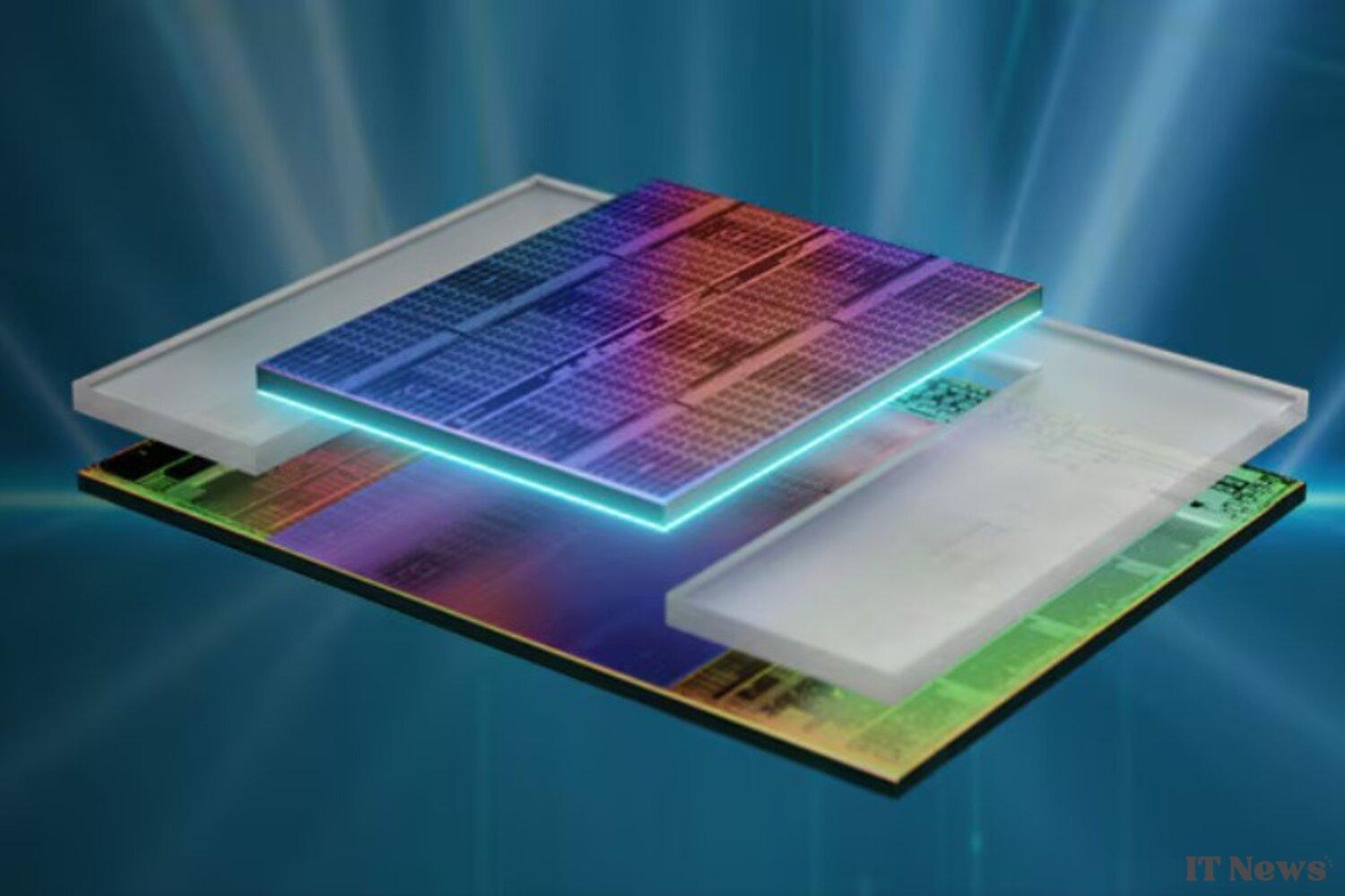
Three-dimensional circuit integration represents a promising avenue for overcoming the current limitations of two-dimensional architectures in the semiconductor industry. But the fabrication of stacked 3D chips, such as some AMD Ryzen processors equipped with 3D V-Cache memory, requires extremely precise and complex lateral and vertical alignment, indirectly increasing their manufacturing cost.
Conventional methods, based on the use of lithographed reference marks and their observation by optical microscopy, show their limits in terms of precision and could prove insufficient for the next generations of ever finer-etched chips. An innovative approach recently developed by a team of researchers at the University of Massachusetts Amherst, however, may offer a promising solution to this technological challenge.
Laser, Holograms, and Metasurfaces
The technique developed by the researchers relies on the use of “metasurfaces” specially designed to serve as alignment marks, combined with a simple system comprising a laser source and a camera. Unlike traditional methods that require direct microscopic imaging of the marks, this new approach exploits the interference of holographic patterns generated by these metasurfaces.
Specifically, when a laser beam illuminates a pair of alignment marks, the transmitted light interacts with the structures of the metasurfaces to create holograms. These then interfere with each other, producing an intensity pattern that is then captured by the camera. Analysis of this interference pattern reveals with sub-nanometer precision the three-dimensional misalignment between the marks, and consequently between the objects – for example, different layers of a microprocessor – on which they are affixed.
The careful design of the alignment marks is at the heart of this technique: their concentric shape with an aperture ring acts as true optical elements, modifying the phase of the incident light to generate the desired holograms. When perfectly aligned, these marks transmit an incident beam without angular deviation. On the other hand, lateral misalignment, even by a few fractions of a nanometer, causes a deviation at different angles, which results in a shift in the holographic patterns. Similarly, an axial misalignment between the marks causes a divergence or convergence of the beams, resulting in a characteristic blur in the observed interference pattern.
Measuring a 3D alignment of a few picometers
The precision achieved by this method is remarkable: simulations have demonstrated limiting accuracies of the order of the laser wavelength divided by 50,000 for lateral misalignment, and divided by 6,300 for axial misalignment. In practice, for a laser operating at a wavelength of 850 nanometers, this corresponds to accuracies of a few picometers for lateral displacement and a few hundred picometers for axial displacement. These levels of precision far exceed the capabilities of conventional methods based on optical microscopy, whose resolution is limited by light diffraction.
Simple, robust and reliable, this new approach also makes it possible to measure three-dimensional misalignment from a single image, which allows for a rapid, real-time alignment process, paving the way for the creation of denser, more efficient and potentially less expensive electronic devices. And this metrology technique based on holographic interference could even find applications in other fields requiring high-precision displacement measurements: the principle of converting a physical displacement into a variation of an optical pattern could thus be exploited to develop displacement sensors – in other words MEMS, or Micro Electro Mechanical Systems – with unprecedented sensitivity.
Source: Nature


0 Comments